Semiconductor
Measurement tasks in the semiconductor industry require highest accuracy and repeatability
Semiconductor
Inspection during the Manufacture of Semiconductors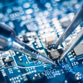
Measurement tasks in the semiconductor industry require highest accuracy and repeatability. Micro-Epsilon offers the right solution for numerous applications from precise machine positioning and wafer inspection to topographic measurements.
Wavefront metrology for Wafer-level optics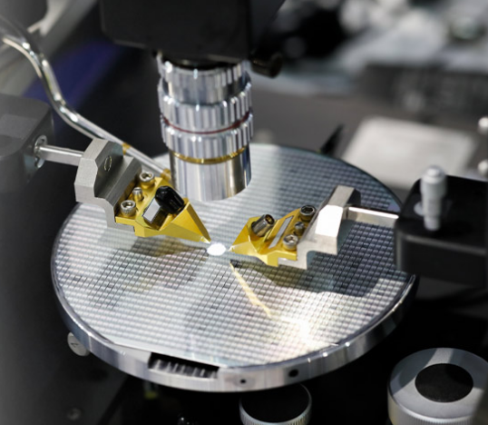
Precise and efficient
When inspecting optics at wafer level, in addition to precision, efficiency is of utmost importance, as a large number of optics must be checked and documented within the shortest possible period of time. Consequently, for reasons of economy, the inspection of wafer-level optics must therefore be automated.
Wavefront measurement technology is applied, for example, to check the image quality of individual lenses that are later used in smartphone lenses. Their tools and master molds are also inspected, e.g. by measuring the 3D surface shape through incident light.
Another example can be found in the inspection of microlenses with diameters down to 50 µm.
Read more